
USB와 같이 differntial signal을 설계시 참고할 수 있는 내용.
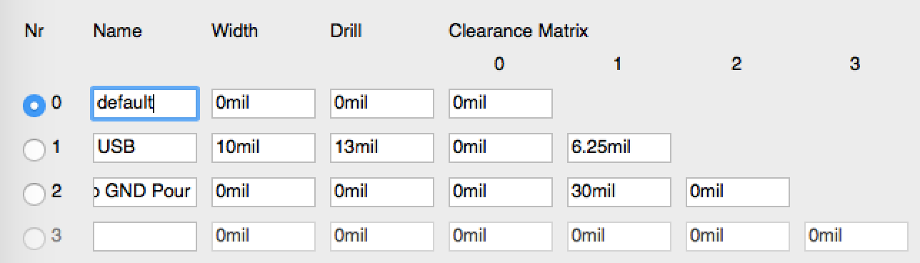
The first step is to create and set net classes. In EAGLE go to Edit->Net classes. There you can create different values for trace width and clearance. Differential pairs should have quite a big clearance to copper pours (2-3 times the track width). Therefore I entered two net classes, one for USB (#1) and one for the top copper pour (#2) as my USB signal is routed on the top layer. As you can see I entered the values from the impedance calculator in net class #1. 10mil for track width. In Clearance Matrix you tell EAGLE how much clearance the different net classes will be used by the Auto Router or differential pair routing. These settings tell EAGLE that USB traces should be separated by 6.25mil and that USB traces should have a clearance of 30 mil to the traces (copper pours) set to net class #2.
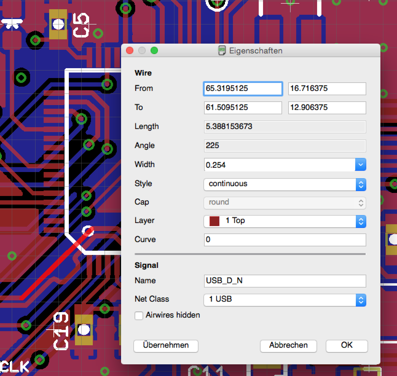
In the next step you have to set the net classes of the traces. I selected each of both USB traces one after the other and set the USB net class in the bottom area of the Info dialog window. Don’t forget to set the Top GND net class to the polygon forming the top copper pour. If you don’t have a top copper pour you don’t need to do that.
참고: http://www.appfruits.com/2015/03/building-your-own-custom-teensy/