한번에 찾기 힘들어서…
May 29, 2018 |
 0 comments
0 comments 0 comments 한번에 찾기 힘들어서…
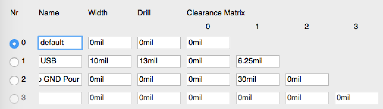
0 comments The first step is to create and set net classes. In EAGLE go to Edit->Net classes. There you can create different values for trace width and clearance. Differential pairs should have quite a big clearance to copper pours (2-3 times the track width). Therefore I entered two net classes, one for USB (#1) and one for the top copper pour (#2) as my USB signal is routed on the top layer. As you can see I entered the values from the impedance calculator in net class #1. 10mil for track width. In Clearance Matrix you tell EAGLE how much clearance the different net classes will be used by the Auto Router or differential pair routing. These settings tell EAGLE that USB traces should be separated by 6.25mil and that USB traces should have a clearance of 30 mil to the traces (copper pours) set to net class #2.
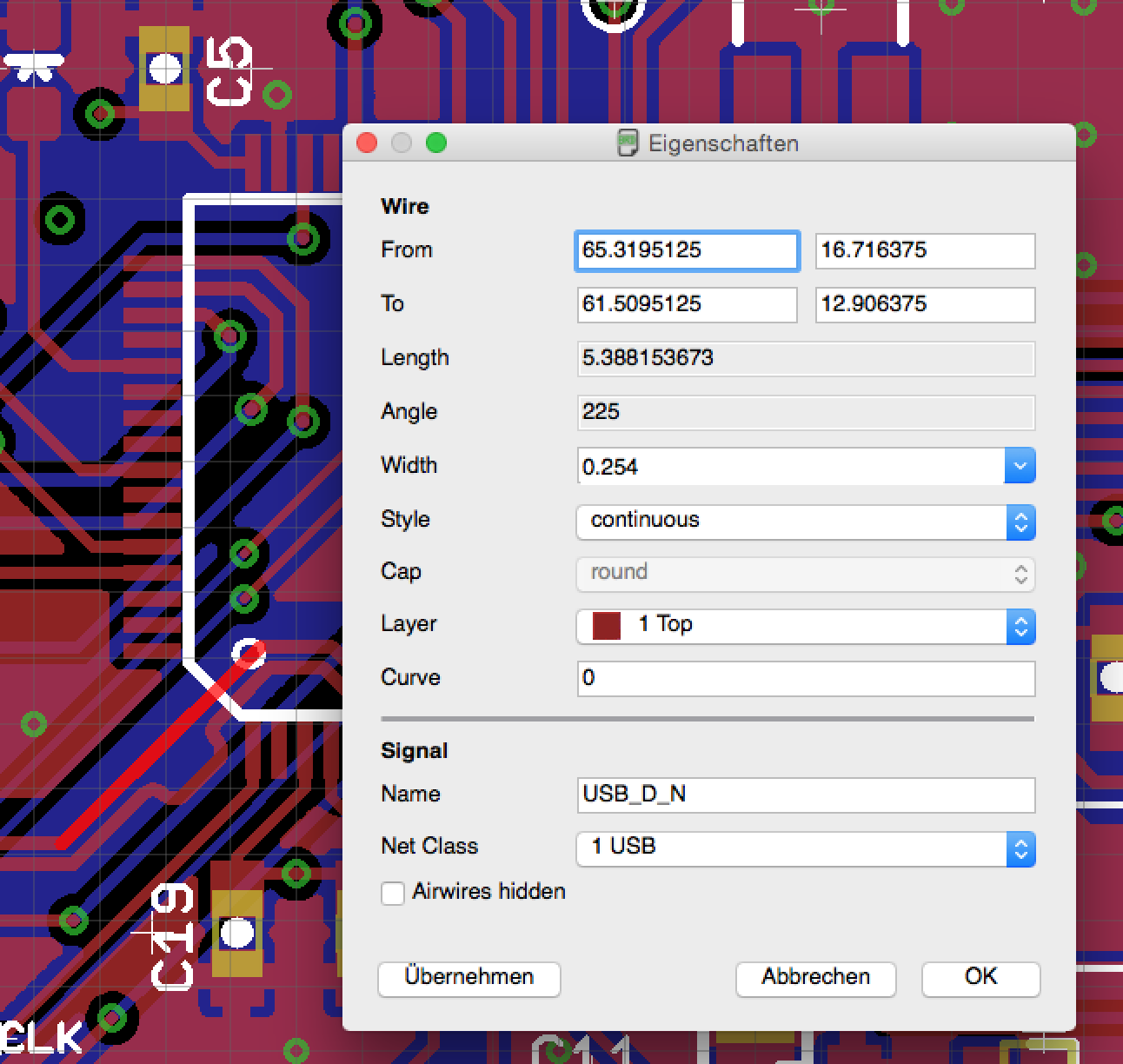
In the next step you have to set the net classes of the traces. I selected each of both USB traces one after the other and set the USB net class in the bottom area of the Info dialog window. Don’t forget to set the Top GND net class to the polygon forming the top copper pour. If you don’t have a top copper pour you don’t need to do that.
참고: http://www.appfruits.com/2015/03/building-your-own-custom-teensy/
0 comments PCB실크를 하나 하나 수정하기는 귀찮은 작업이다. 따라서 다음과 같이 커맨드로 한번에 수정이 가능하다.
1. Smash all parts.
display none tOrigin bOrigin;
group all;
smash (>0 0);
display last;
2. 폰트 변경하기 – 사이즈는 1.27mm, 벡터 폰트, ratio 10%
display none tNames bNames;
group all;
change size 1.27 (>0 0);
change font vector (>0 0);
change ratio 10 (>0 0);
display last;
여기서 “(>0 0)” 는 origin에서 Control-LeftClick 수행한다.
0 comments PCB Design for Manufacturing. – Seeedstudio에서 제공한 문서. PCB업체마다 스펙이 조금씩 다르지만 일반적인 룰은 비슷하므로 참고할 만 하다.
[wpdm_package id=’4186′]
0 comments Eagle CAD는 기본이 2층이라서 4층이상의 PCB설계시 설정변경이 필요하다. 아래그림과 같이 DRC메뉴의 Layers에서 Setup항목의 설정을 (1*16)에서 [2:(1*(2*3)*16):3]으로 변경을 한다. 그러면 레이어가 추가가 된다.

0 comments 키보드의 각 키는 스위치이고 이것의 입력을 받아서 처리하는 MCU는 I/O에 이 스위치가 연결된다. 하지만 모든 키에 I/O를 할당하기 위해서는 키보드의 갯수 만큼 I/O필요하므로 효율적이지 않다. 따라서 키보드 메트릭스 라는 것을 사용한다. 간단히 설명하면 MCU의 I/O에 여러개의 키를 연결하고 주기적으로 키를 스캔하는 방식이다.

위 그림에서 Row R0~R7은 MCU의 입력으로 주기적으로 스캔이되고, Column C0~C19까지는 MCU의 출력으로 5V에 연결이 되어 있다.
키보드 고스트 현상은 여러개의 키가 눌려질때 어떤키가 인식이 안되거나 다른 키가 눌린것으로 인식이 되는 것이다. 아래 마이크로소프트 사이트에서 확인이 가능하다.
아래 그림의 경우 1) a와 c 키가 동시에 눌린경우는 각각의 키가 인식이 된다. 하지만 a, c, b가 같이 눌리는 경우, 보라색의 도통경로가 형성이 되어 d키도 눌린 것으로 인식이 된다. 이런 현상을 방지하기 위해 다이오드가 필요하다.

다음 그림과 같이 각 키에 다이오드를 연결하는데, 스캔 방향이 순방향이 되게 연결을 한다.

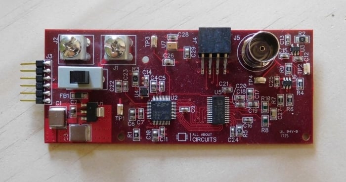
0 comments 0 comments 인덕티브 센서 칩인 TI사의 LDC0851 을 사용한 Tamper detection 응용. 도어가 열리면 인덕턴스 값이 바뀌어 검출이 된다.

참고: https://www.allaboutcircuits.com/projects/tamper-detection-with-inductive-sensing/
0 comments 0 comments